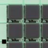
» Semiconductor > Semiconductor Material Marking Equipment > Semiconductor Chip Marking Chip Marking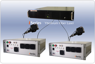 Wafer marking is a requirement within the semiconductor and solar panel industries. Portable digital components, cell phones, PDAs, digital cameras, etc., become smaller and more lightweight but continue to increase in functionality. The Direct Chip Attach (DCA) or flip chip produces a need for wafer identification and tracking. Laser wafer marking has proven to be the best solution, as opposed to ink marking, because it is permanent, readable, and produces a high quality mark fulfilling wafer marking's most stringent requirements.
|
|||||||||||||||
Semiconductor
Semiconductor Dicing and Scribing Equipment
Semiconductor Material Marking Equipment
Semiconductor Wafer Marking
Semiconductor Chip Marking
IC Chip Failure Analysis
Coating Removal
 Member of Semiconductor Equipment and Materials International |
Need a Laser Solution:
Call Us at: Highlighted Application:
Contact Us:
| ||||||||||||||