Display & Semiconductor Systems
Fonon DSS (Display & Semiconductor Systems) engineers and constructs industrial grade systems that use cutting edge laser technologies to drive material processing techniques in the semiconductor and flat panel display industry to new levels. Fonon DSS has demonstrated revolutionary advancements in laser material processing over existing technologies. These advancements translate into numerous cost and performance benefits in a multitude of industries for wafer dicing, flat panel separation, silicon cutting, and direct parts marking used in semiconductor, solar energy, military and defense, flat panel display, automotive, medical, electronics, ceramic and aerospace industries. Fonon has also developed state-of-the-art laser cutting and engraving systems combining flying optics with precision direct drive motion systems for multipurpose cutting and engraving. Our FWLDT® (Fantom Width Laser Dicing Technology®) will cover unprecedented explosive growth and demand in semiconductor markets in China, Taiwan, Japan and Korea. Our unique position and current product recognition in the FPD market worldwide will give us a head-start to become a leader in the FPD and semiconductor industries. A recent change in market disposition opens for Fonon DSS product a wide road to a quarter billion dollar wafer dicing industry.
|
|||||||
Semiconductor
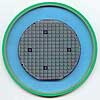
Semiconductor Dicing and Scribing Equipment
Semiconductor Material Marking Equipment
IC Chip Failure Analysis
Coating Removal
 Member of Semiconductor Equipment and Materials International |
Need a Laser Solution:
Call Us at: Highlighted Application:
Contact Us:
|